- 您现在的位置:买卖IC网 > Sheet目录336 > IXS839S1T/R (IXYS)IC MOSFET DRIVER SYNC BUCK 8SOIC
�� �
�
�IXYS�
�IXS839� /� IXS839A� /� IXS839B�
�Synchronous� Buck� MOSFET� Driver�
�Features:�
�?� Logic� Level� Gate� Drive� Compatible�
�?� 2A� Source,� 4A� Sink� Peak� Drive� Current�
�?� Programmable� High-Side� Driver� Turn-on� Delay�
�?� Supports� Floating� Voltage� for� Top� Driver� Up� to�
�24V�
�?� IXS839/839B:� Undervoltage� Lockout�
�?� IXS839A/B:� Output� Shutdown,� Low� Side�
�Shutdown� Inputs�
�?� 10μA� Shut� Down� Current�
�?� 2mA� Quiescent� Current� (Non-� Switching)�
�?� Bootstrapped� High� Side� Driver�
�?� Cross-Conduction� Protection�
�Applications:�
�?� Multiphase� Desktop� CPU� Supplies�
�?� Mobile� CPU� Core� Voltage� supplies�
�?� High� Current� /� Low� Voltage� DC/DC�
�Synchronous� Buck� Converters�
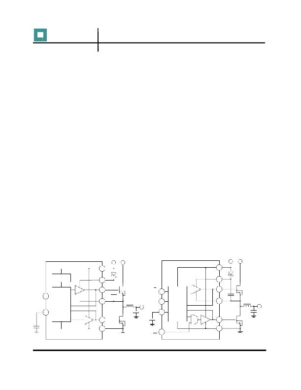
�Figure� 1.� IXS839� Functional� Block� Diagram�
�and� General� Application� Circuit�
�General� Description�
�The� IXS839/IXS839A/IXS839B� are� 2A� Source� /� 4A�
�Sink� Synchronous� Buck� MOSFET� Drivers.� These�
�Synchronous� Buck� MOSFET� Drivers� are� specifically�
�designed� to� drive� two� N-channel� power� MOSFETs�
�in� a� synchronous� buck� converter.� The� High-Side�
�driver� is� powered� via� a� bootstrapped� power�
�connection.� The� driver� is� capable� of� 20ns� High-Side�
�output,� and� 18ns� Low-Side� output� transition� times�
�driving� a� 3000pF� load.�
�The� IXS839� and� IXS839B� incorporate� an�
�undervoltage� lockout� to� prevent� unintentional� gate�
�drive� output� during� low� voltage� conditions.� The�
�IXS83A/B� include� External� Shutdown� and� Low-Side�
�Drive� Shutdown� features.� Simultaneous� shutdown�
�of� both� outputs� prevents� rapid� output� capacitor�
�discharge.� The� high-side� turn-on� delay� is� adjustable�
�with� an� external� capacitor� added� at� the� DLY� pin.�
�The� IXS839/839A/839B� are� designed� to� operate�
�over� a� temperature� range� of� -40°C� to� +85°C.� The�
�IXS839� is� available� in� an� 8-Lead� SOIC,� the�
�IXS839A� and� the� IXS839B� in� a� 10-pin� QFN.�
�Figure� 2.� IXS839A� Functional� Block� Diagram�
�and� General� Application� Circuit�
�5V�
�VIN�
�5V�
�VIN�
�4�
�VDD�
�8�
�VDD�
�UVLO�
�1�
�BST�
�DBST�
�3�
�BST�
�DBST�
�PWM�
�2�
�OVERLAP�
�PROTECTION�
�CIRCUIT�
�8�
�7�
�HGD�
�SW�
�CBST�
�Q1�
�VOUT�
�SD�
�PWM�
�4�
�5�
�OVERLAP�
�PROTECTION�
�CIRCUIT�
�2�
�1�
�HGD�
�SW�
�CBST�
�Q1�
�VOUT�
�DLY�
�3�
�DLY�
�7�
�CDLY�
�5�
�6�
�LGD�
�PGND�
�Q2�
�CDLY�
�9�
�10�
�LGD�
�PGND�
�Q2�
�Copyright� ?� IXYS� CORPORATION� 2004�
�LSD�
�6�
�发布紧急采购,3分钟左右您将得到回复。
相关PDF资料
JLINK-RX-AD
ADAPT BD FOR MINI-JTAG CONNECTOR
JMBADGE2008-B
BOARD JM BADGE
JP9902
CONN JACK MOD INSERT W/O HOLES
JTAGJET-C2000
JTAG EMULATOR FOR TI C2000 MCU
JTAGJET-CCS
JTAG EMULATOR TI C2000/5000/6000
JTAGJET-OMAP3
JTAG EMULATOR OMAP3 W/DEBUGGER
JTAGJET-TRACE-4M
JTAG EMULATOR W/4M TRACE BUFFER
JTAGJET-TRACE-CM3
JTAG EMULATOR CORTEX-M3 1M MEM
相关代理商/技术参数
IXSA10N60B2D1
功能描述:IGBT 晶体管 10 Amps 600V 2.5 Rds RoHS:否 制造商:Fairchild Semiconductor 配置: 集电极—发射极最大电压 VCEO:650 V 集电极—射极饱和电压:2.3 V 栅极/发射极最大电压:20 V 在25 C的连续集电极电流:150 A 栅极—射极漏泄电流:400 nA 功率耗散:187 W 最大工作温度: 封装 / 箱体:TO-247 封装:Tube
IXSA12N60AU1
制造商:未知厂家 制造商全称:未知厂家 功能描述:TRANSISTOR | IGBT | N-CHAN | 600V V(BR)CES | 24A I(C) | TO-263AA
IXSA15N120B
功能描述:IGBT 晶体管 30 Amps 1200V 3.4 Rds RoHS:否 制造商:Fairchild Semiconductor 配置: 集电极—发射极最大电压 VCEO:650 V 集电极—射极饱和电压:2.3 V 栅极/发射极最大电压:20 V 在25 C的连续集电极电流:150 A 栅极—射极漏泄电流:400 nA 功率耗散:187 W 最大工作温度: 封装 / 箱体:TO-247 封装:Tube
IXSA16N60
制造商:IXYS 制造商全称:IXYS Corporation 功能描述:Low V CE(sat) IGBT - Short Circuit SOA Capability
IXSA20N60B2D1
功能描述:IGBT 晶体管 20 Amps 600V 2.5 Rds RoHS:否 制造商:Fairchild Semiconductor 配置: 集电极—发射极最大电压 VCEO:650 V 集电极—射极饱和电压:2.3 V 栅极/发射极最大电压:20 V 在25 C的连续集电极电流:150 A 栅极—射极漏泄电流:400 nA 功率耗散:187 W 最大工作温度: 封装 / 箱体:TO-247 封装:Tube
IXSH 24N60AU1
制造商:IXYS 功能描述:Bulk
IXSH 45N120
制造商:IXYS 功能描述:Bulk
IXSH10N120AU1
制造商:IXYS 制造商全称:IXYS Corporation 功能描述:IGBT with Diode